Category Archives: Uncategorized

I’m Looking Through You : Q&A

In this webinar, we look at the capabilities of TEM and its methodologies. The Q & A from the webinar provides a brief FAQ about this type of analysis.

Q: How large a field of view can you prepare for TEM?

A: While we cannot image the entire prepared sample at once, we typically prepare TEM sections by FIB with an electron transparent region that is about 10 µm in length. We actually prefer an area that is smaller than that just to maintain mechanical stability, but that’s the typical limit of FIB preparation. In a TEM sample that is prepared by ultramicrotomy, an ultrathin sample can be up to 2 or 3 mm in diameter.


Q: Can any material be prepared for TEM?

A: Most likely not. There are some restrictions around what we can put into the transmission electron microscope. Again, the most important restrictions are that it needs to be vacuum compatible and that it needs to be able to stand up to the FIB preparation if we go the FIB route. However, some polymer samples that may be vacuum compatible might be ‘sectionable’ with our ultramicrotome but may degrade under an electron beam. Some could even be too soft to section by ultramicrotomy. There are many, many materials that can be used for TEM, however.


Q: Can TEM be used to measure crystallinity index as XRD?

A: In a single crystal sample, we get well-resolved diffraction patterns that we can use to measure lattice parameters and similar aspects of crystallinity.


Q: Is EDS analysis in the TEM or STEM more time consuming than in the SEM?

A: The answer to that question is no. It typically takes about the same amount of time once you have your sample in the instrument to actually generate the EDS analysis.


Q: Can you do grain boundary imaging and analysis in the TEM?

A: Typically, the answer to that question is yes. Again, it can be somewhat sample dependent, but the huge advantage in the TEM or STEM is that the sample is so thin that there is virtually no spot blooming compared to bulk EDS analysis in the SEM, allowing us to perform EDS analysis on a nanometer rather than micron scale. So if you have a problem along those lines, again, we would certainly encourage you to get in touch with us and we can see about designing an analysis to address that.


Q: Can you do grain or particle size analysis from TEM images?

A: Again, the answer to that, in general, is yes. However, you will need to contact us to confirm.


Q: Can you make a TEM sample from a four-inch wafer?

A: Yes. On a four-inch wafer, if there are small structures or small defects that we need to find, the capability exists to drive to those positions and then excise those regions of interest from the wafer as lift-out samples and prepare them for subsequent TEM analysis.


Q: What is the difference between high resolution TEM and STEM?

A: STEM in its name implies that you are scanning the beam: Scanning Transmission Electron Microscopy. In that technique, we would form a finely focused probe beam, step it across the sample in a raster fashion to generate the image (as is done in an SEM) but we take advantage of the higher beam voltages and different electron optics to provide additional signals and information about samples, as compared to SEM. In a high resolution TEM image or TEM in general, the beam is not scanned; we rely on the electron optics to form a global image of the sample, much as you would in a light microscope.

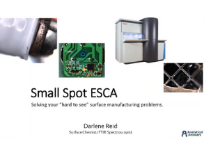
Small Spot ESCA : Q&A

The above webinar discusses analyzing surface chemistry on micro-devices and its methodologies. Here you can examine a Q & A from the webinar of FAQs about this type of analysis.

Q: Does surface roughness have an effect on depth profiles?

A: Surface roughness does indeed have an effect on depth profiling. But with our new instrumentation, our ability to rotate a sample at multiple points coupled with our better charge neutralization helps to mitigate the effects that you would see from surface roughness. It may cause your sample to sputter etch at a bit slower rate than expected, but rotating will help decrease the effects that we see from that. Charge neutralization also helps to mitigate the effects one sees. So yes it’s possible, but there are caveats.


Q: How deep can you profile? How long does it take to sputter?

A: That depends on the sputter rate of the material under analysis. Again, we do a quality check four times a year on our instrumentation. And we know that silicon dioxide sputters at a rate of 10 nanometers per minute in our instrumentation. We have parameters that can increase or decrease that sputter rate and make it much faster or much slower, but if that’s a benchmark, it’s limited. Thus, with the 10-nanometer sputter rate, it just limits how deep we can get into the sample.

And some materials may sputter faster or slower, so it all depends on how much time you want to spend to get, say, a micron into the surface.

Something to keep in mind as you’re sputtering past a micron is that interfaces may be intermingled as you’re getting deeper into the surface because of the crater that’s being created. It depends on the data that can be collected, as well as the electronics, and the set-up of the instrumentation. Those are all factors to keep in mind as you’re sputtering one to two to three microns into a sample. Time is a big factor– how long do you want to spend to sputter a micron or more into your sample.

It’s possible, and we can do it. But once you get into the two to three micron range, there are several things to keep in mind. You may see artifacts as we sputter that deep into the sample. As long as you remember that there may be artifacts and that that data may have to be taken with a grain of salt, you can sputter as deep as you want, as long as you have the time to do it.


Q: Can you give me an example of when weight percentage analysis would be needed?

A: Weight percentage analysis is often needed when a client comes in with an idea of a product that’s been on the surface. It’s not always possible, but sometimes they say, hey, we know the weight percent of this product. Can we see some of that as we analyze our sample? So let’s say we have a particular product of poly dimethyl silicone, and can we see that reflected on our sample. Sometimes that can be calculated to weight percent that can be found. Weight percentage can also be useful or beneficial if you’ve tried to create a product similar to a competitor’s and you want to see if that works out. Sometimes that can be back calculated. Sometimes that comes with a caveat.


Q: How can you produce maps and line scans similar to what you showed in your depth profiling system?

A: A map is actually made up of multiple points so we analyze each point and software will combine the data to give it to you. So you are losing some sensitivity to data because it is a multidimensional analysis. We recommend doing a point analysis to get your overall composition. We take multiple points, and just like a pixelated picture the software combines all those pixels.

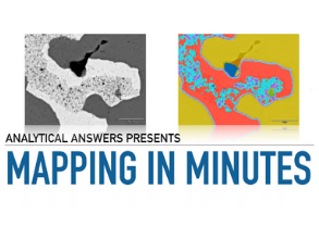
Fast Mapping : Q&A

The above webinar discusses the capabilities of fast mapping and its applications. Here you can read the Q & A from the webinar for a series of FAQs on the topic of fast mapping.

Q: Do you have to define elemental windows before starting the map?

A: The answer is no. Because you’re getting an entire spectrum from each pixel in the map, you don’t have to define anything ahead of time or after the fact – that’s locked in. You can always go back and change the elements you’ve mapped for, so that way you can dynamically change it as needed. You can even add elements partway through. You can subtract them if you find that they don’t make sense because they shouldn’t be there. But again, if you don’t agree with the spectrometer, you can always check your work by extracting synthesized spectra containing the same elements, and verifying that any decisions that you came to are actually accurate and correct.


Q: Is this method able to be used for polymer or non-metallic materials?

A: The answer is yes. You can certainly use this to look at polymeric materials. As with all SEM work on polymers, you typically have to coat the sample with a conductive coating. Otherwise, you will end up with charging problems because the sample cannot dissipate the charge from the electron beam.


Q: How deep into the sample does the beam penetrate?

A: The beam penetrates anywhere from one up to tens of microns, depending on the density of the material and the energy of your beam. The scale in the webinar example is 10 microns in the lateral dimension, but the same holds true in the vertical direction. Thus, when you’re hitting a low atomic number material like aluminum with a 30 kilovolt beam, most of the information will come from the outermost few microns but you can still get some data from much deeper into the sample surface. So if you’re looking for very sensitive detection, you can still pick up those very weak traces of elements when they’re coming in from a distance. As you can see with the iron comparison, the penetration depth is much smaller because of the higher atomic number of that material. And so you also get a smaller analytical volume with most of the information coming from the top 2 microns. But you can still get some data from as deep as 5 microns, but it’s not the highest intensity data that’s coming from the fringes of those “spot blooms” where the e-beam spreads out into the material.

Pollen

The nice spring weather has come and gone. With that nice spring weather also came pollen…everywhere! Although it is often seen as a nuisance for triggering allergies, pollen is very interesting to look at magnified. You may be surprised at how different various pollen types look.


The familiar yellow haze on our cars and everywhere else can be annoying. But the variation in the appearance of different types of pollen at higher magnifications can be surprising.

Pollen close up:


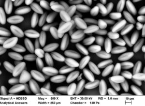
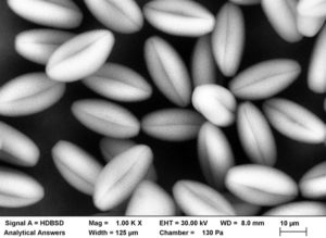
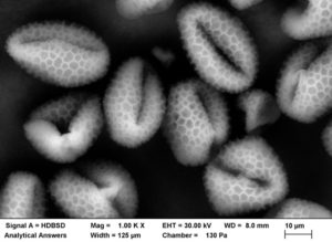
Empress Tree Flower Pollen – This tree (Paulownia tomentosa) produces a small grain size pollen with a “bean” or “seed” shape and longitudinal folds.

Empress Tree Flower Pollen 2 – While the wall surfaces appear smooth at lower magnifications, a mottled appearance begins to appear at higher magnification.
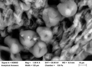
Gala Apple Blossom Pollen – The pollen grains shown here are still seated on the anther surface. They are quite large with a smooth wall surface, and appear almost “fluffy” with only a few folds.
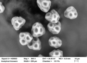
Pink Azalea Pollen – These are relatively large pollen grains with a faceted wall structure.
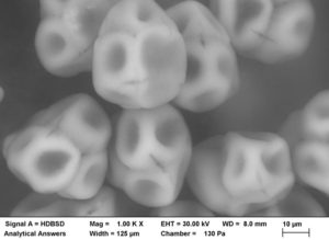
Pink Azalea Pollen 2 – At higher magnification, the wall surface has the appearance of connected groups of dimpled facets with a “stitch” that connects the facets.
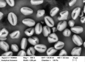
Russian White Lilac Pollen – These medium-size grains have a mottled wall surface with one or two folds.

Russian White Lilac Pollen 2 – At higher magnification the folds on some grains actually look like holes. The wall surface texture is also clearly visible.


Webinar Recap: Anywhere Services Live

Did you miss our final webinar before the summer – Anywhere Services Live? Don’t worry, you can learn everything that you missed right here in this blog post or you can watch the recorded version on demand here:

http://analyticalanswersinc.com/anywhere-services-live/

This May webinar was a bit different from our traditional webinar format. Analytical Answers recently celebrated our 25th anniversary of providing microscopy, spectroscopy and other materials analysis services. In honor of this, Joseph Bedard, Senior Failure Analysis Scientist; Jay Powell, Senior FTIR Spectroscopist; and Edward Norton, Technical Director at Analytical Answers presented this session on one of the unique services the company offers. This webinar focused on our Anywhere Services, which allows you to send in your samples regardless of where you are, and have our team of professionals analyze them with your participation. This service can be partially or entirely live, depending on the needs of the client.

Ed Norton, Technical Director, started off the presentation by introducing the Analytical Answers Anywhere Service, which Analytical Answers has been providing to clients for over a decade. By participating with the scientists as they are performing an analysis, clients can ask questions and see certain parts of the process in greater detail. As an added bonus, clients can bring in colleagues and vendors of their choice at their convenience so that they can see the analysis in real time and work in collaboration.

The sample that was analyzed in this webinar was chosen from client submissions. It was a circuit board from a medical device that failed Highly Accelerated Life Testing (HALT). This is a testing procedure that combines temperature cycling with high humidity, while putting the sample under stress (powering it up) to see how prone it is to failure. Viewing the sample circuit, soot and burned components were clearly visible as well as various residues. Sites on the back side of the board also showed evidence of contamination and possible corrosion as well as a burned area of a component.

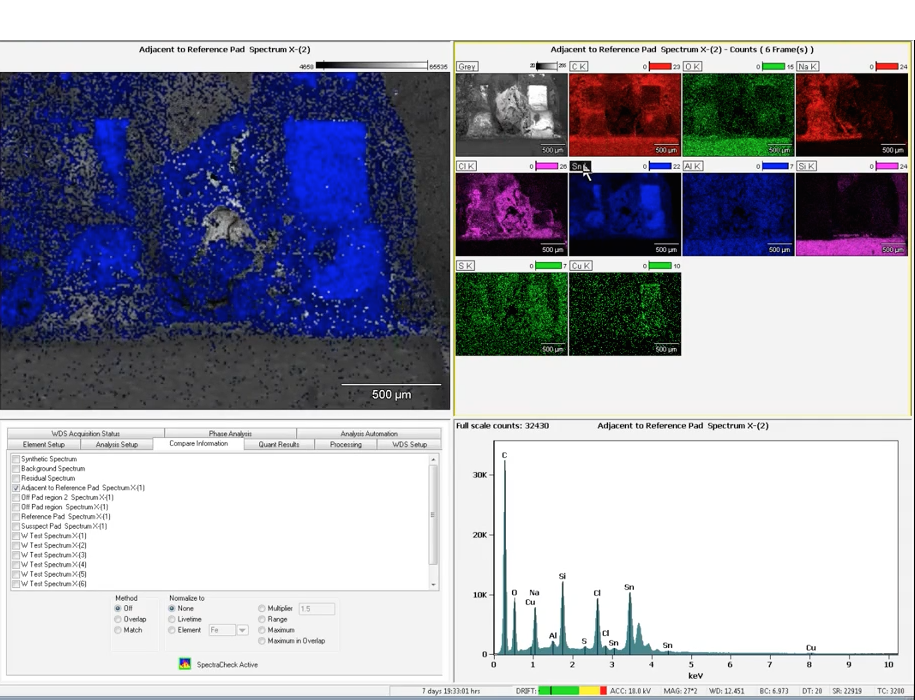
Joe Bedard examined areas of suspected corrosion using Scanning Electron Microscopy (SEM) with Energy Dispersive X-ray Spectroscopy (EDS) to identify the elemental composition of those areas. Joe used a very helpful feature of the instruments he was using, which is the ability to take an optical image of the sample and, using optical and SEM imaging, quickly perform a 3-point stage registration. This correlative approach allows one to navigate to any part of the sample in the SEM by double-clicking on a point of interest on the saved optical image.

Next, Joe focused his analysis on several small areas that appear to have been particularly damaged, one possibly forming a bridge between device leads. He also analyzed lead itself and some material that could be a flux residue near the lead. He collected secondary and backscattered electron images (which show surface topography and atomic number contrast, respectively) as appropriate to minimize charging artifacts in the images, and X-ray spectra from each region. One of the EDS spectra in particular showed a significant amount of chlorine, which may indicate there was a corrosive species present during the HALT process. Chlorine was also detected in other parts of the damaged board, but was not found on the reference lot board while analyzing a similar area.

Joe then collected a quick EDS elemental map of the analyzed region to understand the distribution of the elements detected in the previous analyses. This is a key piece of information in understanding whether this particular material created a bridge between adjacent contacts causing a short circuit. By collecting the elemental map, Joe was able to determine that tin was indeed forming a bridge between two contacts on this device, and was probably the cause of the unit failure during the HALT process. The chlorine component is the likely cause of the observed corrosion.

Jay Powell, Senior FTIR Spectroscopist, then took over the analysis, using Fourier Transform Infrared Spectroscopy (FTIR) to examine the organic compounds that may be present (as indicated by the large amounts of carbon [C] detected by EDS). He commented that, while EDS detected carbon and oxygen on a certain component, that technique does not show chemical composition – which is where FTIR comes into the process. Using a portion of the board that was not used for SEM work, he collected a small amount of the glossy material from the surface of the failed part for his analysis. He also took a sample of flux from the “control” board for comparison. Since the FTIR microscope can target a small area of a sample for analysis, a large specimen is generally not needed and a small sample is often either physically removed or solvent-extracted from a larger part.

By comparing the sample from the failed board to that from the reference board under similar background conditions, it was clear that not all components were the same. This led to the conclusion that what appeared to be flux on the failed board was not the same flux material collected from the reference board.

Through the use of complementary analytical techniques such as SEM/EDS and FTIR, it showed that there were significant differences in the flux from the failed board, compared to the reference board. The presence of an incorrect flux with the presence of chlorine, likely resulted in the corrosion and eventual short circuit of the board.

And with the Anywhere Services by Analytical Answers, clients and vendors can take part in this intricate analysis process to gain a better understanding of both the analytical process and the practical information they gain through detailed analysis – without having to be present in the laboratory.

Careers in STEM: Education and Outlooks


Careers in Science, Technology, Engineering and Mathematics (STEM) have been the fastest growing fields for years now. The employment growth, median wages, and growth opportunities are well above most other fields. “The future of the economy is in STEM,” says James Brown, the executive director of the STEM Education Coalition in Washington, D.C. “That’s where the jobs of tomorrow will be.”

In fact, employment occupations in STEM related fields are expected to grow more than 9 million between 2012 and 2022, and while this is a general projection for all STEM fields, the occupations with the most employment growth are related to technology, math or engineering. Workers in STEM fields earn an average median wage of about $76,000 per year, which is more than double the median wage for all workers.

“STEM offers a cooperative, innovative, and exciting work environment that is unparalleled,” says Aimee Kennedy, vice president for education and STEM learning at Battelle Memorial Institute in Columbus, Ohio.

But how do these “jobs of tomorrow” begin? How do we ensure that more people will choose to go into these fields and contribute great things to the scientific community and society as a whole?

It all begins with education. Preparing for STEM careers can begin as early as high school, and successful STEM workers recommend pursuing challenging courses, such as Advanced Placement (AP) math and science courses, to improve your transcript and prepare for the challenges of STEM work or by taking advantage of free online coding courses.

Most STEM careers require a Bachelor’s degree, and that’s to start. Although a Bachelor’s degree will help you master one field, many career advisors recommended that you use college electives to study other STEM related courses. There are many great careers open to Bachelor’s recipients, despite the common belief that “everyone needs a Ph.D.” Some examples of STEM jobs that require a Bachelor’s are actuaries, civil engineers, and information security analysts.

More advanced jobs, including those in research, usually do require a Master’s or Doctoral degree. A Master’s degree usually requires an additional one to three years after undergraduate study, and most programs require students to write a research paper, known as a thesis paper. Some STEM careers that require a Master’s degree are epidemiologists, hydrologists, and statisticians.

A Doctoral degree usually requires anywhere from three to five additional years after undergraduate study, and students often have to complete a dissertation, which is a lengthy research paper that contributes new knowledge and ideas to their field. Examples of occupations in STEM fields that require Doctoral degrees include animal scientists, computer and information research scientists, and physicists.

Although many jobs require these lengthy studies, there are some STEM related careers that only require an Associate’s degree, and a few require either some college but no degree or a high school diploma or equivalent. An Associate’s degree only requires two years of study, and some examples of occupations in STEM fields that only require an Associate’s  include chemical technicians, computer network support specialists, and mechanical drafters.

Work experience in a related field is usually recommended, and sometimes required, for certain STEM careers. Even if your desired occupation does not require experience, it will help to set you apart and help you develop valuable skills before you start. Students need to look for internships and volunteer opportunities while they are still in school. Additionally, getting STEM experience can help you determine exactly what field you want to go into.

Although STEM careers can often be challenging, the rewards far outweigh the disadvantages. Challenges that STEM workers have to face vary depending on the field, but usually involve applying for funding for research, juggling different priorities, navigating government regulations and stressing about deadlines. Despite these downsides, STEM careers often entail problem solving, repeating and refining those problem solving steps, experimentation,  building models and using various tools to push ideas from the imagination and turn them into a reality.   It also involves writing proposals, so writers and creatives are necessary in the world of STEM to think of new and innovative ways to convey scientific concepts in a way everyone can understand.

STEM workers report being respected and fulfilled. Working in a STEM field will usually mean that you will work on something interesting and meaningful. Most STEM workers find their jobs intellectually stimulating, and they enjoy collaborating with people who share their enthusiasm for science.

Most STEM fields also include rapid change, so the professional development is very dynamic. “There’s always something more to learn,” says Julie Herrick, a volcanologist at the Smithsonian Institution National Museum of Natural History in Washington, D.C. “Don’t expect an end.”

“You feel that what you’re doing is important and you matter as an employee,” says Frances Tirado, a mathematical statistician at BLS in Washington, DC. “People value your skills, listen to your ideas, and think that what you do is magic.” With all these great rewards, advantages, outlooks, and growth, it’s easy to see why careers in STEM are the fastest-growing career field today.

However, according to the Department of Education, only 16% of all High School Seniors are interested in pursuing a STEM career. In order for our society to thrive off our great scientific discoveries and contributions, we need more scientists and engineers. And in order to do so, we need to get children more interested in science and other related subjects–the earlier the better!


Sources:

https://www.nsf.gov/statistics/seind14/index.cfm/chapter-1/c1h.htm

http://money.cnn.com/2014/09/25/smallbusiness/stem-facts/

https://www.bls.gov/careeroutlook/2014/spring/art01.pdf